Energy Bands in Conductors:
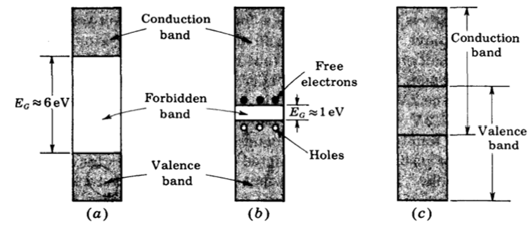
Metals like copper, aluminum we can see no forbidden gap between the valence band and conduction band. The two gaps cover. Subsequently, even at room temperature, an enormous number of electrons are accessible for conduction. So with no extra energy, such metals contain an enormous number of free electrons and subsequently called great conductors.
In a conductor (metal) – The valence and conduction bands cover, so for all intents the energy gap is zero. Therefore, electrons need a small amount of energy to remain in the conduction band and lead electricity.
Energy Bands in Insulators:
If there should arise an occurrence of such protecting material, there exists a huge forbidden gap in the middle of the conduction band and the valence band. It is inconceivable for an electron to hop from the valence band to the conduction band. Subsequently, such materials can’t lead and called insulators. The forbidden gap is wide, roughly of around 7 eV is available in encasings. For a jewel, which is a protector, the forbidden gap is around 6 eV. Such materials may direct just at high temperatures or if they are exposed to high voltage. Such conduction is uncommon and is called a breakdown of an encasing.
The energy band structure of at the ordinary grid separating is shown schematically in the picture below. For a diamond (carbon) gem the locale containing no quantum states is a few electron volts high (EG ==: 6 eV). This enormous forbidden band isolates the filled valence locale from the empty conduction band. The energy which can be provided to an electron from an applied field is too small to even consider carrying the molecule from the filling into the vacant band. Since the electron can’t secure adequate applied vitality, conduction is unimaginable, and consequently, the jewel is a cover.
Energy Bands in SemiConductors:
The forbidden gap in such materials is restricted as appeared in a picture. Such materials are called semiconductors. The forbidden gap is about in such materials, the vitality given by the warmth at room temperature is adequate to lift the electrons from the valence band to the conduction band.
A substance for which the width of the taboo vitality area is moderately little (- 1 eV) is known as a semiconductor. Graphite, a crystalline type of carbon yet having a crystal evenness which is diverse 4 5!g. from diamond, has such a little estimation of EG, and it is a semiconductor. The-4 most significant down to earth semiconductor materials are germanium and silicon, which have estimations of EG of 0.785 and 1.21 eV, separately, at O°K. Energies of this size typically can’t be obtained from an applied field. Consequently, the valence band stays full, the conduction band vacant, and these materials are separators at low temperatures. Be that as it may, the conductivity increments y4th temperature, as we clarify beneath. These substances are known as inherent (pure) semiconductors