Junction transistor, transistor action, characteristics of a transistor and transistor as an amplifier (common emitter configuration), the basic idea of analog and digital signals, Logic gates (OR, AND, NOT, NAND and NOR)
Junction transistor:
The bipolar junction transistor (BJT) is worked by three doped semiconductor territories disengaged by two p-n junctions Region, emitter, base, and collector. The two kinds of BJTs are, the npn and pnp. The two junctions are named the base-emitter junction and the base-collector junction. All together for the transistor to work appropriately, the two junctions must have the right dc inclination voltages
- – the base-emitter (BE)junction is forward one-sided
- – the base-collector (BC) junction is switch one-sided
Transistor action:
The term transistor activity alludes to the control of the huge collector-emitter (connecting) current by the littler base (back injection) current in forwarding dynamic activity, the starting point of “current increase” in a BJT. Two highlights of the gadget are fundamental for transistor activity
- a limited base, which powers all electrons infused from the emitter to traverse the base nonpartisan area to the collector.
- a high producer doping contrasted with the base doping, making base (electron) injection the prevailing term
Characteristics of a transistor:
The presentation of the transistor in a circuit relies upon the V–I attributes of the transistor. A transistor is a three-terminal gadget. One terminal is made normal to output and input. The other two will be the other output terminal and the input terminal. Because of which terminal is made normal, we have.
- Common base
- Common emitter
- Common collector configurations
Transistor as an amplifier (common emitter configuration):
Normal Emitter Amplifier setup of NPN transistor is known as a Class A Amplifier. A “Class A Amplifier” activity is one where the transistors Base terminal is one-sided so as advance inclination the Base-emitter junction. The outcome is that the transistor is continually working somewhere between it is cut-off and immersion areas, consequently enabling the transistor speaker to precisely recreate the positive and negative parts of any AC info sign superimposed upon this DC biasing voltage. Without this “Bias Voltage” just a single portion of the info waveform would be intensified. This regular emitter amplifier setup utilizing NPN transistor has numerous applications yet is ordinarily utilized in sound circuits, for example, pre-amplifier and power amplifier stages.
Basic idea of analog and digital signals
Analog Signal
An analog signal is a nonstop wave signified by a sine wave (presented underneath) and may shift in sign quality (amplitude) or recurrence (waves per unit time). The sine wave’s amplitude value can be seen as the higher and lower points of the wave, while the frequency value is measured in the sine wave’s physical length from left to right.
![]()
Digital Signal
A digital signal – an unquestionable requirement for PC preparing – is depicted as utilizing paired (0s and 1s), and thusly, can’t take on any partial qualities. As showed in the realistic underneath, advanced sign hold a uniform structure, giving a steady and reliable sign. Due to the characteristic unwavering quality of the digital signal, innovation utilizing it is quickly supplanting an enormous level of simple applications and gadgets.
![]()
Logic gates (OR, AND, NOT, NAND and NOR)
Digital systems are said to be developed by utilizing logic gates. These gates are AND, OR, NOT, NAND, NOR. The fundamental activities are portrayed beneath the guide of truth tables.
AND gate:
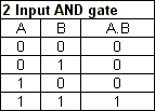
The AND gate is an electronic circuit that gives a high yield (1) in particular if every one of its information sources is high. A dot (.) is utilized to demonstrate the AND activity for example A.B. Remember that this dot is once in a while excluded for example A.B

OR gate :
The OR gate is an electronic circuit that gives a high yield (1) if that at least one of its sources of input are high. A plus (+) is utilized to demonstrate the OR activity


NOT gate:
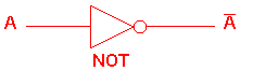
The NOT gate is an electronic circuit that delivers an altered variant of the contribution at its output. It is otherwise called an inverter. On the off chance that the information variable is A, the modified output is known as NOT A. This is additionally appeared as An’, or A with a bar over the top, as appeared at the output. The graphs underneath show two different ways that the NAND logic gate can be arranged to create a NOT gate. It should likewise be possible utilizing NOR logic gate similarly.


NAND gate:
This is a NOT-OR gate which is equivalent to an OR gat pursued by a NOT gate. The output of all NOR gates is high if any of the information outputs are low.

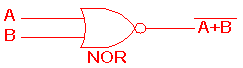
NOR gate:
This is a NOT-OR door which is equivalent to an OR gate pursued by a NOT gate. The output of all NOR gate is low if any of the information inputs are high.
.