Semiconductors
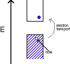
Semiconductors have a small energy gap between the valence band and the conduction band. Electrons can make the jump up to the conduction band, but not with the same ease as they do in conductors.
Semiconductors consist of small gap in between conduction band and valence band. The conduction electrons can jump over the band, but not with that much ease as they jump in conductors.
Two types of semiconductors are there:
- Intrinsic semiconductors
- Extrinsic semiconductors
Intrinsic Semiconductors
An internal semiconductor or an undoped semiconductor or i-type semiconductor refers to a semiconductor in its pure form. When every electron jumps into CB, the missing electron will result in generating a hole which can freely move in VB. In this semiconductor, the number of holes are just same as the jumped number of electrons.
Semiconductor’s sample in its purest form is known an intrinsic semiconductor. The content of impurity in the intrinsic semiconductor is very much small, in the order of – one in 100 million parts i.e. 1/100 million parts of a semiconductor.
Extrinsic Semiconductors
In the case of Extrinsic semiconductors, the band gap or the energy gap is intentionally controlled by adding small impurities in the material. This process is known as “doping”. Adding impurities or doing doping in the lattice can change lattice’s electrical conductivity and thus, semiconductor’s efficiency varies.
In the extrinsic semiconductors or the doped semiconductor, the number of holes are not as same as the number of electrons that jump.
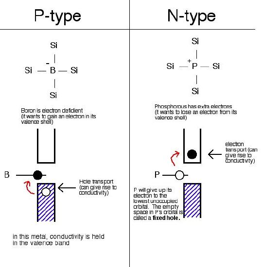
Two different types of extrinsic semiconductors are there, positively charged doped P-type and negatively charged doped N-type.
The extrinsic semiconductor that is doped with an electron donor atom is known as the N-type semiconductor, as most of the charge carriers in crystal have negative electrons.
The acceptor of electron dopant is the atom that accepts the electron from lattice, to create a space (vacany) where the electron must be referred to as the hole; a hole that can move like a positive charges particle via crystal.
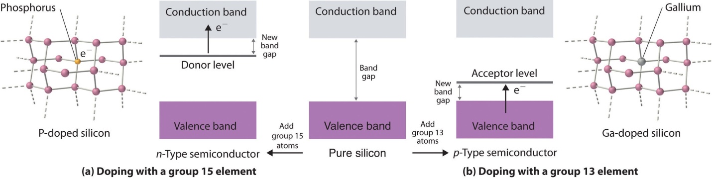
The extrinsic semiconductor, which are doped along with electron receptor atom is known as a P-type semiconductor, as most of the charge carriers in crystal contain positive holes.
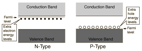
Energy Band Gap and hole energy between V and C
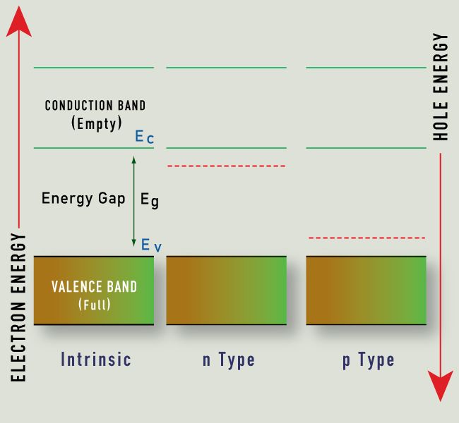
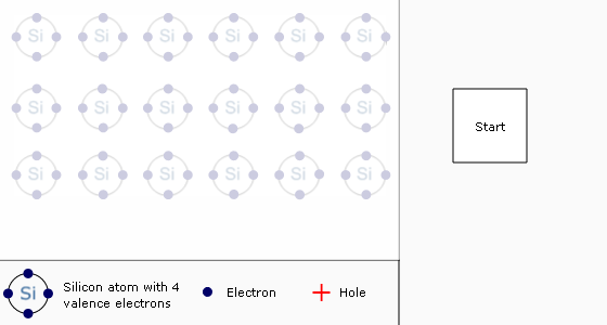
Those solids whose conductivity is situated between insulators’s and conductors’ conductivity, are called semiconductors. On contrary to metals, the conductivity rises with the rise in temperature. Also, because of electrons’ exchange, so as to attain the “ noble gas configuration”, the semiconductors do arrange in the form of lattice structure.
With increase in temperature, it results in generation of free electrons and breaking of bonds.
Silicon lattice’s cut out
On the basis of semiconductor’s conductivity properties, the electron flow is decided. The diagram above of electron band describes why these semiconductors act in this manner.